Introduction
Computational Electrodynamics is the process of modeling the interaction of electromagnetic fields with physical objects and the environment. The ACMS has developed a range of state-of-the-art simulation codes for solving 3D time domain and spectral vector Maxwell equations. The software we develop employs the most advanced and computationaly effcient methods and are used to tackle a diverse set of problems from all areas of electrostatics and electrodynamics.

Photonic crystal microcavity
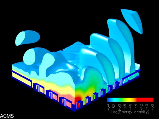
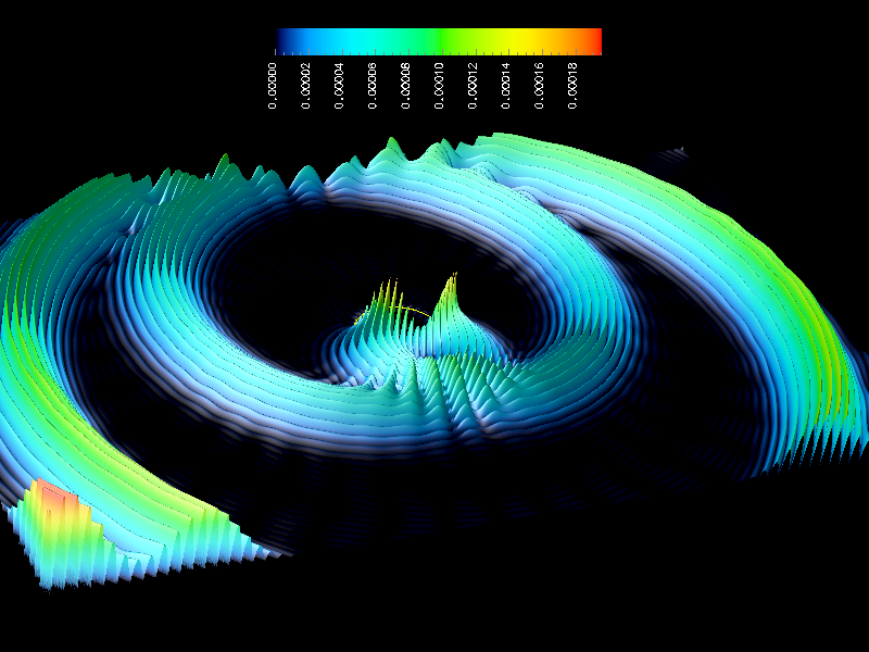
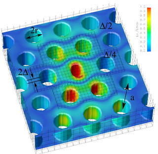  We examined the practical problem of computing the quality factor, Q, of a photonic crystal microcavity. Emission from the microcavity in the direction perpendicular to the plane of the crystal exhibits a strong sensitivity to small geometry dislocations of the lattice. We examined the practical problem of computing the quality factor, Q, of a photonic crystal microcavity. Emission from the microcavity in the direction perpendicular to the plane of the crystal exhibits a strong sensitivity to small geometry dislocations of the lattice.
A change in lattice dislocation equal in size to one coarse grid cell results in a several times increase of the quality factor. To accurately resolve the lattice dislocation two levels of grid refinement are used.
The refined grids are placed such that they provide the highest resolution in the dislocation region where the predominantly Ex-polarized mode of the cavity (X-dipole mode) has high electric field intensity.
For a dislocation size equal to two coarse grid cells the dislocation is resolved with eight grid points on the finest grid with cell size. The improvement in the computation time is a factor of ten, compared to the computation on the uniform grid with the resolution of the finest grid.
References
- C Dineen, "Time Domain Simulation and Visualization of the Near-Field Electromagnetic Distribution Around Dielectric and Metal Nano-Structures", International Workshop on Theoretical and Computational Nano-Photonics, TaCoNa-Photonics 2008, Physikzentrum, Bad Honnef, Germany
- A.R. Zakharian, M. Brio, C. Dineen and J.V. Moloney, "Second order accurate 3D FDTD space and time grid refinement method", Phot. Tech. Lett. 18(11), pp. 1237-1239, 2006
- A.R. Zakharian, M. Brio, C. Dineen and J.V. Moloney, "Stability of 2D FDTD algorithms with local mesh refinement for Maxwell's equation" Comm. Math. Sci. 4(2) (2006)
- J.V. Moloney, A. R. Zakharian, C. Dineen, and M. Brio, "AMR FDTD solver for nanophotonic and plasmonic applications", Proc. SPIE 5451, 97 (2004), DOI:10.1117/12.548983
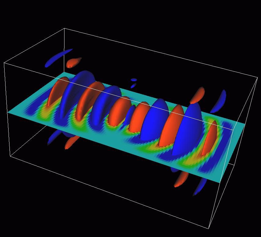
Normal mode coupling in photonic crystal nanocavities
 High quality photonic crystal structures can be realized by a periodic arrangement of air holes in a dielectric medium. Introducing apropriate defects into the structure makes it possible to design optical microcavities with mode diameters in the wavelength range and very high Q factors. High quality photonic crystal structures can be realized by a periodic arrangement of air holes in a dielectric medium. Introducing apropriate defects into the structure makes it possible to design optical microcavities with mode diameters in the wavelength range and very high Q factors.
 These microcavities are well suited to study non-perturbative light-matter coupling effects if one inserts an appropriate optically active system into the cavity. At the ACMS we investigated a microcavity structure with a single defect into which we placed a two-level atom which is resonant with the predominant cavity mode. These microcavities are well suited to study non-perturbative light-matter coupling effects if one inserts an appropriate optically active system into the cavity. At the ACMS we investigated a microcavity structure with a single defect into which we placed a two-level atom which is resonant with the predominant cavity mode.
In order to answer this question, we not only have to compute the electromagnetic field in and around the photonic crystal structure, but also model its excitation by a classical light source in the far field. The light-matter interaction inside the microcavity has to be computed self-consistently and the far field components of the transmitted and/or reflected fields as well as the corresponding spectra have to be evaluated.
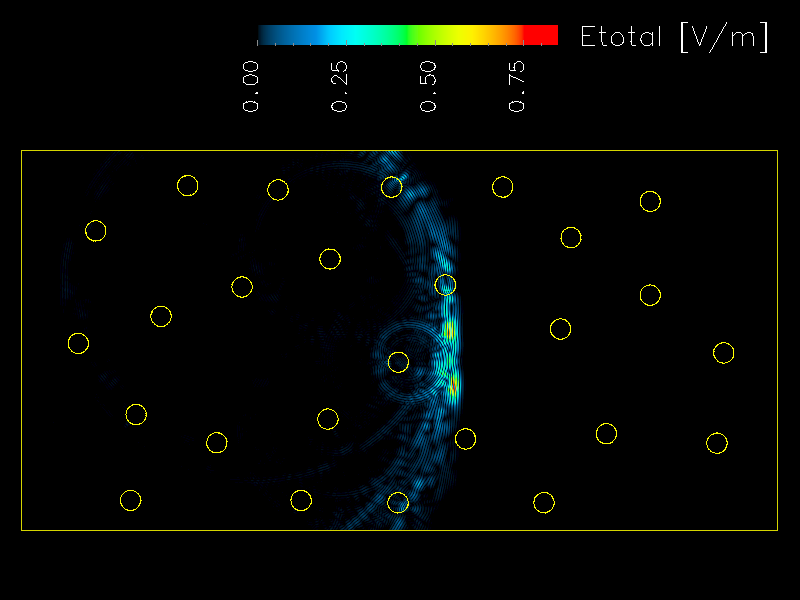
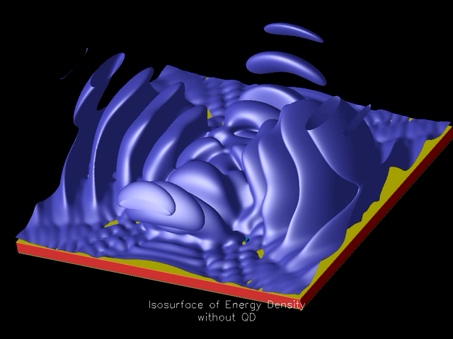 We investigate strong light-matter interaction and normal mode coupling/splitting in a system composed of a single two-level atom and the localized mode of a small mode volume photonic crystal nanocavity. We investigate strong light-matter interaction and normal mode coupling/splitting in a system composed of a single two-level atom and the localized mode of a small mode volume photonic crystal nanocavity.
Our results illustrate the near-field and radiative properties of the electromagnetic field for the nanocavity and the perturbative effects of introducing a resonant atom into the cavity. By numerically seperating the field structure into evanescent and propagating components we show that, even though the cavity modes are strongly localized around the defect, each mode has a well defined component that travels into the far field from which the mode-atom coupling signatures (normal-mode splitting) may be observed.
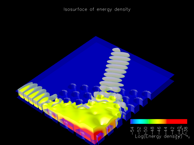 The simulated system consists of a 2D photonic crystal slab of semiconductor pattered with a triangular lattice of air columns. A localized defect mode is formed in the crystal lattice by reducing the radius of a single hole resulting in a small mode volume nanocavity into which a two-level atom is placed. The simulated system consists of a 2D photonic crystal slab of semiconductor pattered with a triangular lattice of air columns. A localized defect mode is formed in the crystal lattice by reducing the radius of a single hole resulting in a small mode volume nanocavity into which a two-level atom is placed.
The electromagnetic field dynamics of the system are simulated using a three dimensional FDTD method and the optical response of the atom is modeled within the density matrix framework using a fourth order Runge-Kutta solver to numericaly integrate the differential equation for the microscopic polarization.
References
- C. Dineen, J. Förstner, A. R. Zakharian, J. V. Moloney, and S. W. Koch, "Electromagnetic field structure and normal mode coupling in photonic crystal nanocavities," Opt. Express 13, pp. 4980-4985, (2005)
- J. Förstner, C. Dineen, A. R. Zakharian, J. V. Moloney, and S. W. Koch, "Normal Mode Coupling in Photonic Crystal Nanocavities," in Frontiers in Optics, OSA Technical Digest Series (Optical Society of America, 2005), paper FWC2.
Pulse scattering in dispersive media
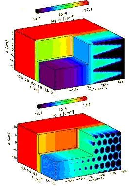
At the ACMS we simulated light propagation through densely scattering media using the Finite Difference Time Domain. Our work is mainly concerned with the effects of multiple scattering. In particular we are interested in the deformation, temporal stretching, attenuation, and spatial spreading, of ultra short optical pulses.
Multiple scattering of ultra short oprtical pulses by aerosols, dust, and water droplets in clouds or fog is responsible for a number of deleterious effects which severely impact the performance of imaging, remote sensing, lidar, and optical communication systems.
This research is also relevant to light scattering from biological cells for medical diagnostic imaging. We used the FDTD to model how light interacts with tissue at the cellular level and determine scattering patterns. Of particular interest is the backscattering component which may be used to determine quantitative information about cell size and size distributions.
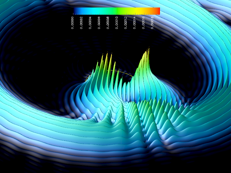
This animation [3.0Mb] shows a 10fs Gaussian pulse scattering from a single 3.0Micron water disk. A portion of the initial pulse is captured and excites a number of whispering gallery modes at the interface. These modes form a pair of counter propagating pulses that slowly radiate to the external environment. This animation [3.4Mb] shows a close in view of the formation of the whispering gallery modes and their decay.
When multiple scatters are present in the domain the optical pulse undergoes multiple scattering events which may result in a large backscattered component. In this animation [5.9Mb] the 10fs pulse encounters a random distribution of 3.0 micron diameter water disks.
Note that the color legend scale is dynamically re-normalized to the maximum field amplitude in the computational domain. After the main pulse has exited the right hand side of the computational domain the backscattered component becomes visible.
Electrical/Thermal Transport in Semiconductor Heterostructures
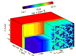 Carrier and heat transport from the contacts through to the active layer within a semiconductor heterostructure play a critical role in determining the useful operatingrange of high power edge- and surface-emitting semiconductor heterostructures.
We have developed a fully 3D simulation of diverse high power devices using the full time-dependent drift diffusion equations coupled to Poisson s equation. The simulation allows us to investigate different designs for optimizing high brightness diode laser sources including various surface outcoupling geometries.
Contact profiling (pictures on the right) has been proposed as a means of mapping the current flow in the active layer to a preferred optical mode profile. Computed current profiles and thermal profiles in the active layer act as inputs to our interactive supercomputing simulation. We are also investigating coupling the classical carrier transport to a fully nonequilibrium quantum transport within the barrier and QWs of the active structure.
|